Wave Photonics has developed a core computational design technology to characterise and model an integrated photonics fabrication process and then generate a Process Design Kit with fabrication-tolerant, high-performance components.
01
Foundry process data
02
Proprietary fabrication model fitting
03
Parallel automated design
04
Fabrication tolerant, low-loss PDK
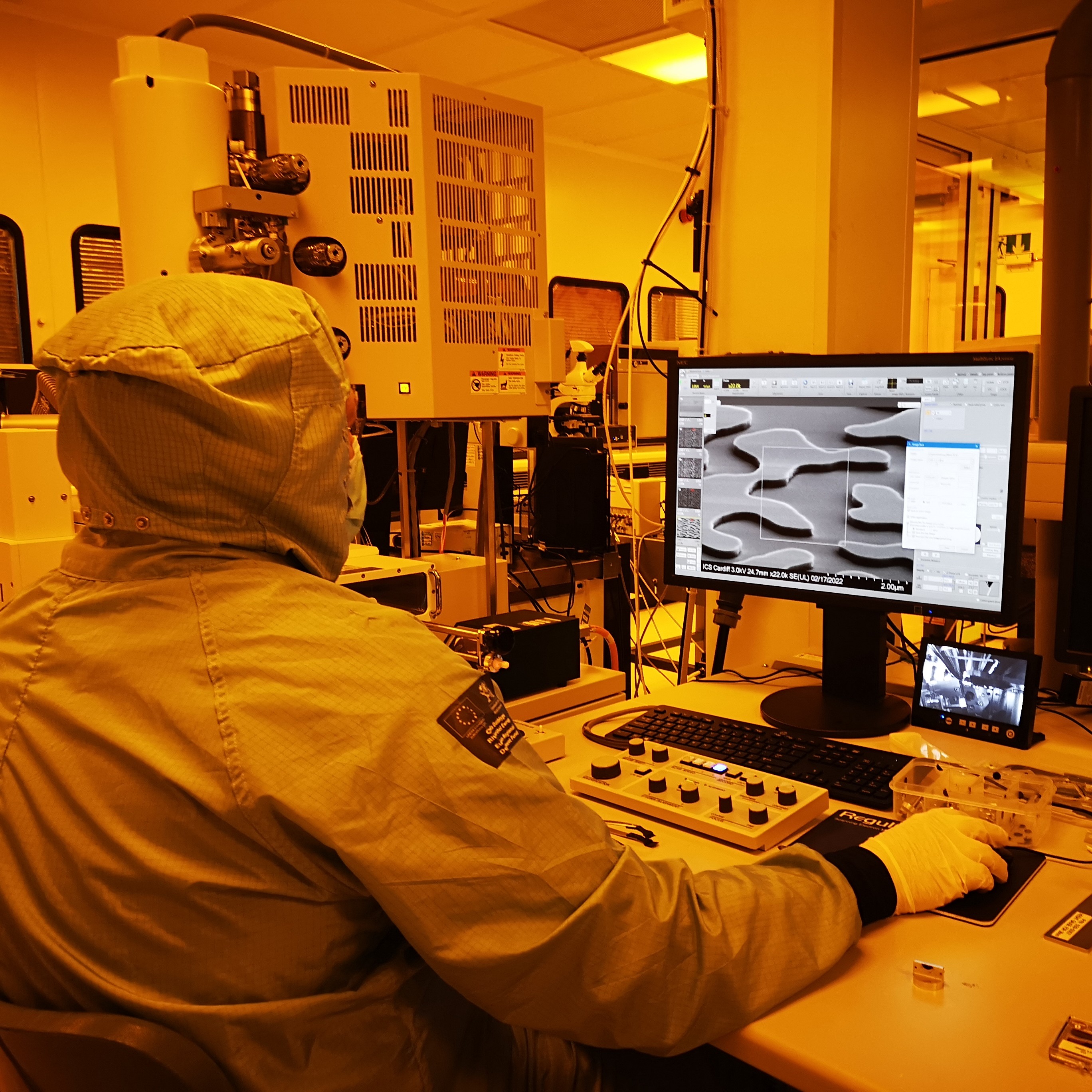
Process Characterisation
We gather measured process data to fit our fabrication model.
Enables first-time right design
Fabrication-tolerant components for improved yield
Process improvement with rapid component re-adaptation
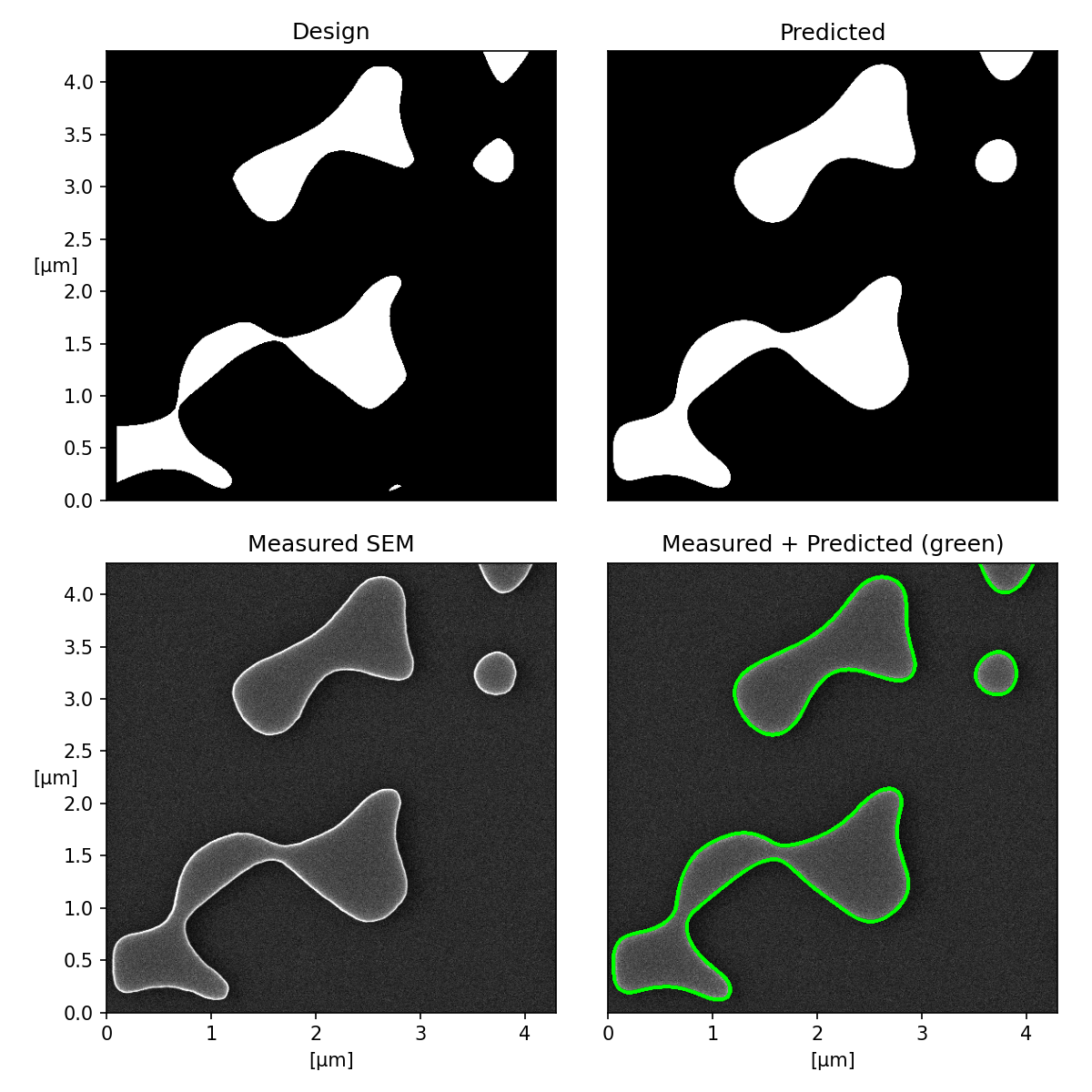
Fabrication Model
Our fabrication model captures the statistical distribution of possible photonics device shapes resulting from the fabrication process.
Validated proprietary physics and data driven model for first-time right component design
Advanced statistical modelling enabling optimisation with respect to measured process variation
Access real expected component performance in circuit simulation before tape-out
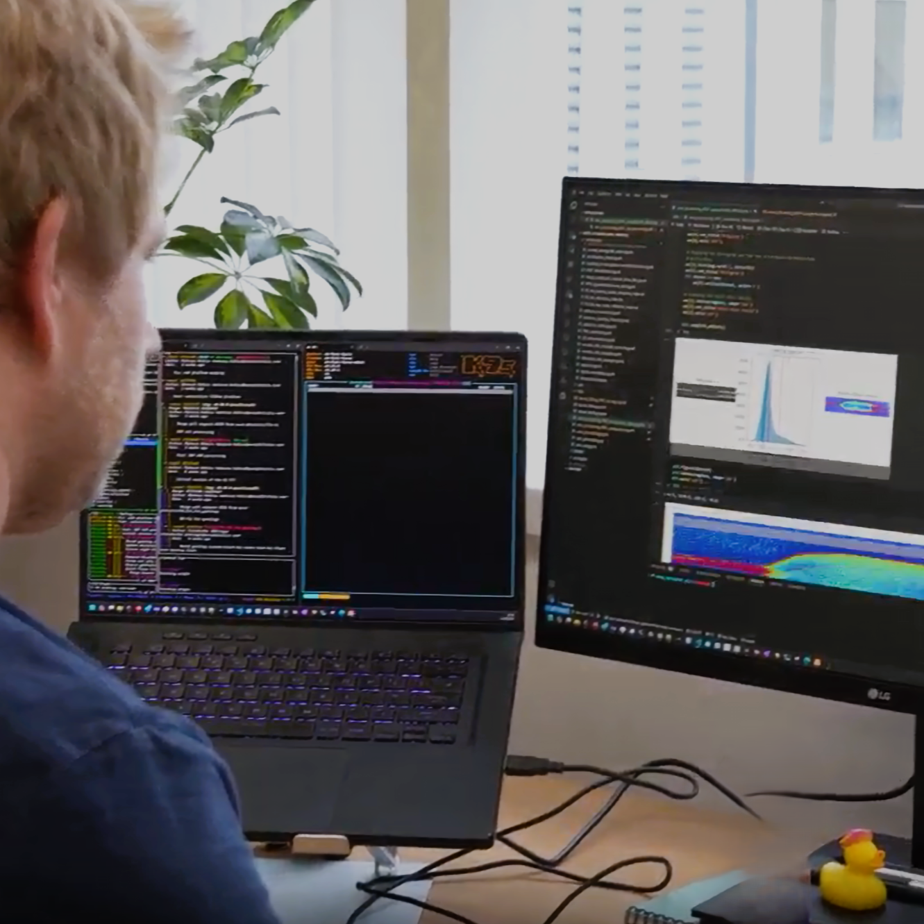
Automated Design
Our cloud-scalable infrastructure which can run with thousands of simulations in parallel enables automated design of fabrication-tolerant building-block libraries.
Rapid component design for new fabrication processes or new wavelengths, serving a wider range of applications
Get to volume faster with reduced design iteration time
Expansive building block libraries for every process or wavelength supported
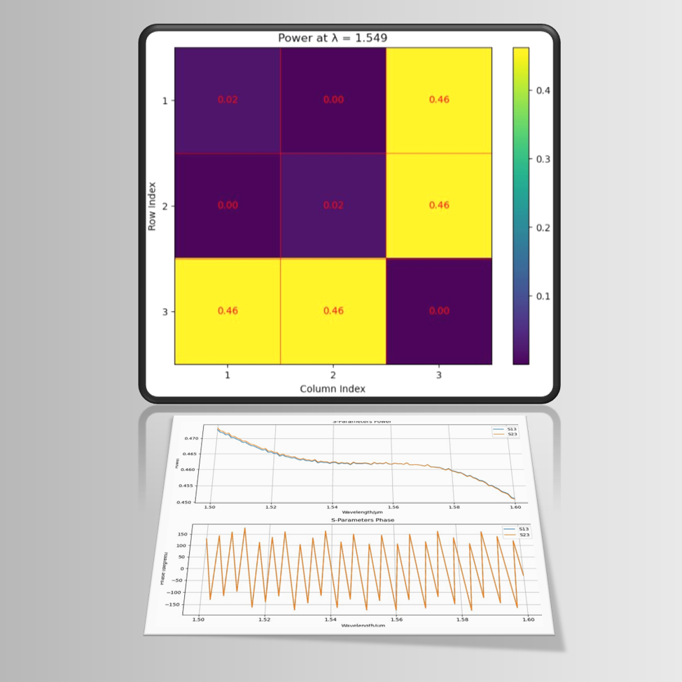
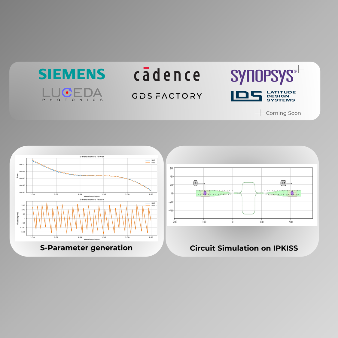
Scattering Parameters
Our PDKs come with fabrication-aware scattering parameters to allow for full circuit simulation before taping out a chip.
Get more accurate simulation results of the expected component performance on a given fabrication process
Predict before fabrication how a given circuit is expected to perform
Assess the suitability and performance of components
EDA Integrations
We have built integrations to make our PDKs accessible with various EDA tools.
Streamlined route to developing PICs by incorporating Wave Photonics' pre-designed and expansive component library into available EDA tools
Our EDA Integrations are compatible all the features on offer by the EDA tools, allowing you to work in your workflow with ease
Range of EDA tools available and expanding
PDK Management Platform
Our PDK Management Platform for foundries can streamline the designer experience by ensuring foundry PDKs work with the expanding range of EDA tools we have built integrations for, and come with ready-calculated S-parameters for circuit simulation.
We enable rapid, fabrication-tolerant PDK development. Explore our offerings for your next integrated photonics product and reduce your PIC development time.
Find out more about our PDKs for your PIC applications.


.JPG)