We offer easy-to-use reusable PIC packaging templates & Assembly Design Kits (ADKs) which minimise custom development requirements and costs. With our QPICPAC offering, you can have packaged photonic chips in as little as one month.
Our photonic packaging templates & ADKs can help to minimise custom development requirements and costs.
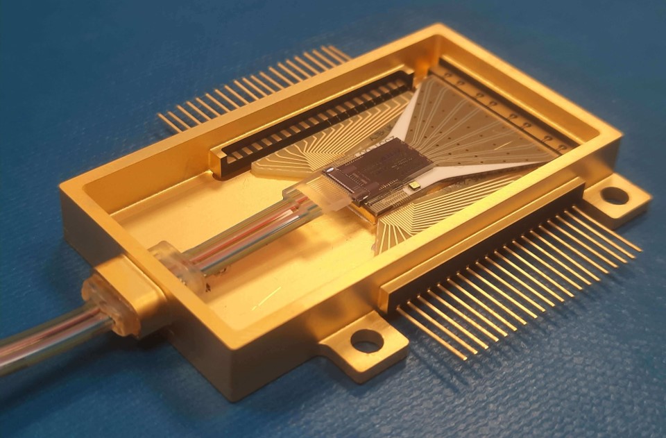
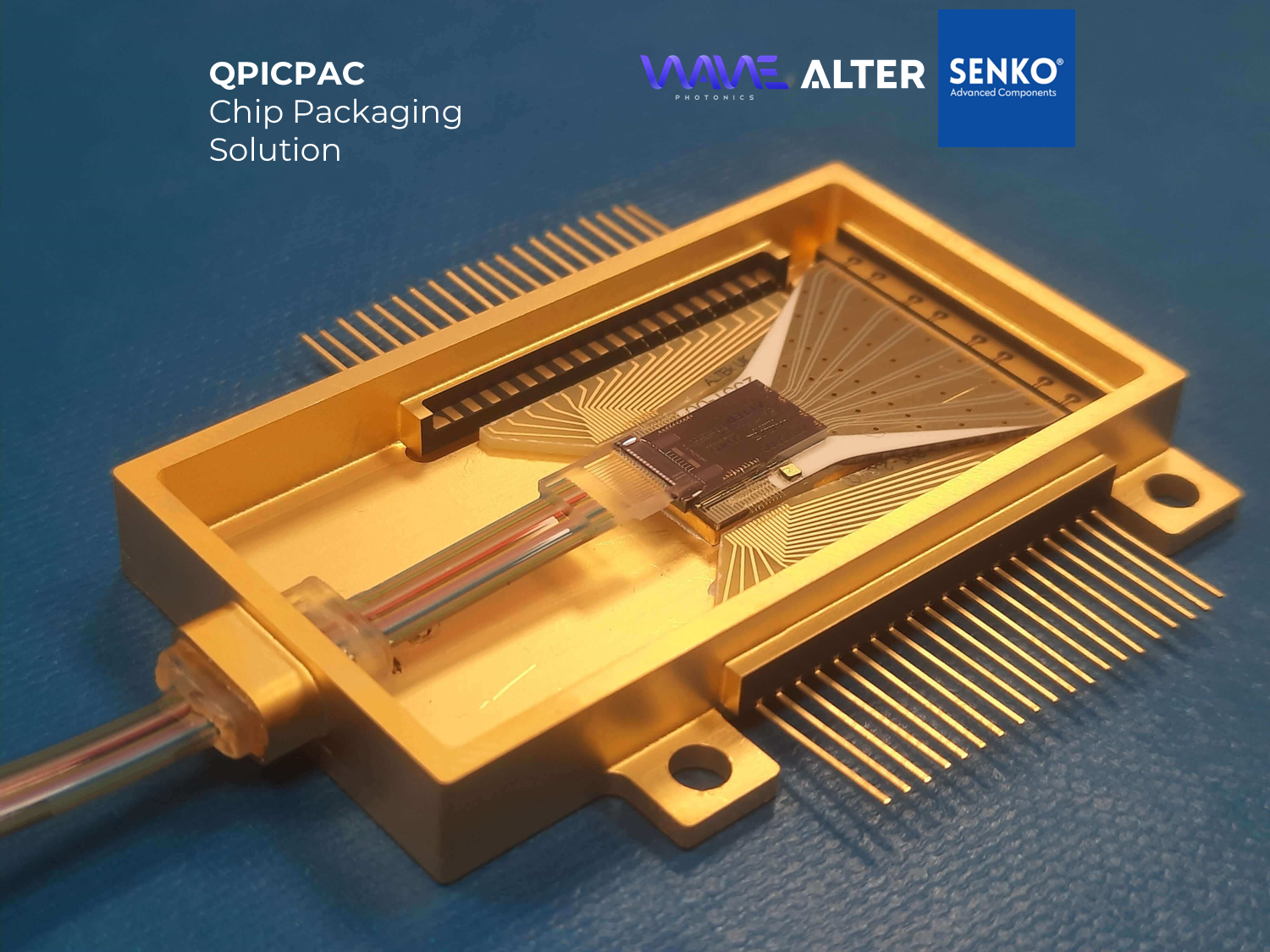
QPICPAC - Chip Packaging Solution
Our QPICPAC offering, an easy-to-use reusable PIC packaging solution, was developed working with SENKO Advanced Components, a company producing high-quality optical components, and Alter Technology, who offer advanced packaging solutions. This PIC packaging solution provides a template-driven approach to minimise custom development requirements and costs. For more information, please sign up to our platform or contact us.
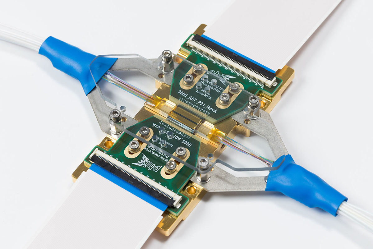
PHIX Characterization Package Template
Wave Photonics provides easy-to-use photonic chip packaging templates for the PHIX Characterization Package solution. These templates are available for both the CORNERSTONE SOI 220 nm passive and active fabrication processes. We have packaging templates available for Wave Photonics’ PDK of optimised components as well as CORNERSTONE open-source PDKs. For more information, please sign up to our platform or contact us.
Packaging protects your chips mechanically, can provide inbuilt temperature control and consistent optical coupling to your chip. Chips that are not designed for packaging may be either expensive (e.g. 10s of £ks) or rather impossible to package as you want to.
Using our standardised packaging templates can offer several benefits to chip designers compared to custom packaging.
01
Save time on chip design
Using our standardised packaging templates which are already suited for packaging, can save time while designing your chips, both in terms of reducing time with considering the suitability of designs for packaging, and in designing the packages themselves.
02
Cheaper PIC Development
Using a pre-designed package solution offers a cheaper alternative to custom packaging and also reduces the risk of an inability to package chips properly.
03
More predictable behaviour of packaged chips
Standard approach gives repeatability, so it's much easier to plan how well your packaged chip will behave (e.g. speed of electrical RF connections and the optical coupling loss to expect).
04
Quicker Packaging Process
A standard approach means the packaging company can order standard packaging elements more easily and may already have the right elements in stock leading to a quicker packaging process.
QPICPAC Solution & Pricing
Packaging your chips provides a scalable approach to interact with your chips, and keeps your chip more protected. Our QPICPAC offering provides an easy-to-use turnkey packaging solution for prototyping and R&D.
Wave Photonics, SENKO Advanced Components, a company producing high-quality optical components, and Alter Technology, who offer advanced packaging solutions, worked together as part of an Innovate UK project referred to as Quantum Photonic Integrated Circuit PACkaging (QPICPAC), to produce packaging solutions for Quantum Photonic Integrated Circuits (QPICs).
The packaging solution, which includes design templates and components, can minimise custom development requirements and costs for quantum technology companies.
QPICPAC is also suitable for many other different prototyping applications.
PHIX provides an assembly and packaging service for photonic integrated circuits (PICs). They support chip prototypes as well as high-volume manufacturing.
Wave Photonics provides easy-to-use photonic chip packaging templates for the PHIX Characterization Package solution. These templates are available for both the CORNERSTONE SOI 220 nm passive and active fabrication processes.
We have packaging templates available for Wave Photonics’ PDK of optimised components as well as CORNERSTONE open-source PDKs.
How to package your chips with our packaging templates
Save time and reduce costs by packaging your next chips with our packaging templates.
Design
Design your chip using our packaging template.
01
Contact us
Provide information such as the number of chips and fabrication run.
02
Screening
We ensure the design is suitable for packaging.
03
Tapeout & payment
All consumables ordered now to avoid delays.
04
Chips ready
Chips go directly to packaging company for packaging.
05
Packaged chips
Receive your packaged chips.
06
We enable rapid, fabrication-tolerant PDK development. Explore our offerings for your next integrated photonics product and reduce your PIC development time.
Find out more about our PDKs for your PIC applications.


.JPG)