Wave Photonics launches PIC Testing Services and TDK on the PDK Management Platform
April 14, 2026
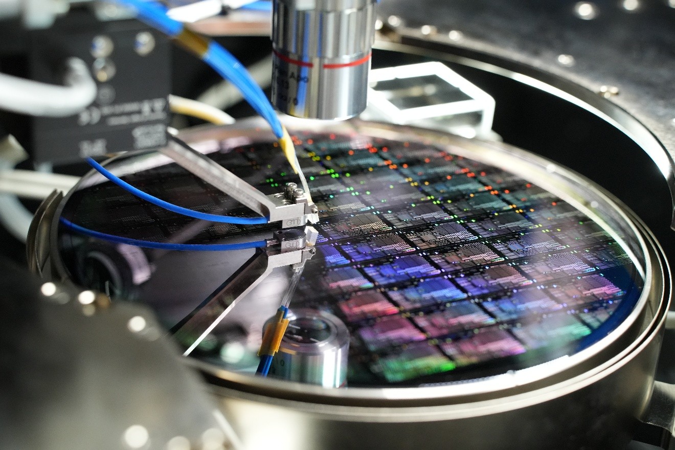

Automated optical probing setup showing fibre array alignment to a photonic die for wafer-scale characterisation
Wave Photonics has launched PIC testing services and a Test Design Kit (TDK) on the PDK Management Platform, expanding the platform's complementary services across the photonic design, validation, and packaging workflow.
The service supports high-throughput, parallelised measurement and performance analysis for passive photonic integrated circuits (PICs) at both die level and wafer scale. It complements existing capabilities available through platform partners, helping designers move more efficiently from design to fabrication, testing, and packaging within a connected ecosystem
Our services support:
• 100 mm, 150 mm, and 200 mm wafer-scale testing
• Passive PIC characterisation at 780 nm and 1500-1630 nm
• Up to two-week turnaround for wafer scale measurement and analysis
• Compatibility with our QPICPAC packaging service, enabling wafer-level testing to identify the best dies before packaging
The measurement outputs include raw spectra, fitted curves, and wafer-level statistical analysis, providing detailed insight into device performance and variability.
The TDK defines the layout and design requirements needed to design chips for reliable optical characterisation using Wave Photonics’ probing infrastructure. By making these requirements accessible through the platform, we enable designers to account for testing earlier in the design process, reducing design iterations and improving first-time success.
Explore the testing services and access the TDK on the PDK Management Platform: pdk.wavephotonics.com
For active devices, chip-scale testing, or custom measurement workflows, contact us at info@wavephotonics.com


.JPG)