Wave Photonics Brings CEZAMAT’s Silicon Nitride Integrated Photonics Process to its PDK Management Platform
June 9, 2026
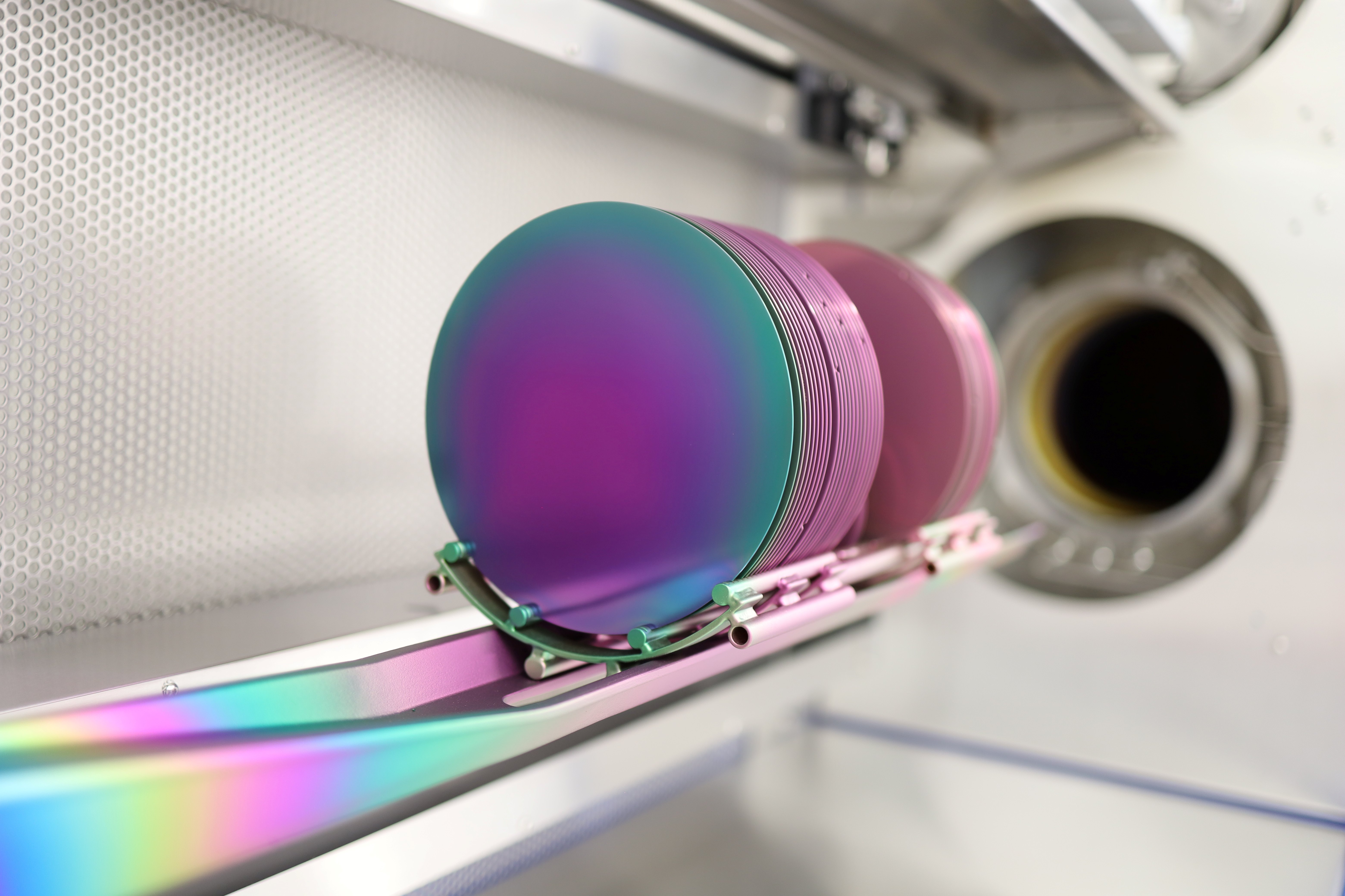

Wave Photonics announces that CEZAMAT, a network of specialised laboratories in Poland, has made its Silicon Nitride (SiN) PDK available to PIC designers across all the major EDA tools through Wave Photonics’ PDK management platform. Designers can now download CEZAMAT’s SiN PDK from the PDK Management Platform and use it in their preferred layout environment. CEZAMAT’s PDK is available at pdk.wavephotonics.com.
The addition of CEZAMAT’s SiN process to the platform makes an important photonics capability more accessible. Silicon nitride is widely used for datacoms and optical networking because of its low propagation loss properties, and is increasingly becoming an important enabler of emerging applications in quantum technologies and sensing, where visible and near-infrared wavelengths are required.
As Europe’s integrated photonics ecosystem is growing rapidly, easier access to foundry processes can help accelerate that momentum. More accessible processes help create a flywheel: designers can move from concept to fabricated PICs more efficiently, foundries can reach a wider range of designers, and applications in areas such as quantum technologies, sensing, datacoms, and optical networking can develop faster. Over time, this broader access can help the ecosystem grow more quickly.
Wave Photonics’ PDK Management Platform helps foundries make their processes accessible to a wider community of PIC designers by distributing their PDKs across all the major EDA tools.
Key features of the platform include:
Marcin Lelit, CEZAMAT’s PDK Designer, said, “We are proud to strengthen the European photonics ecosystem with our first public PDK. This is just the starting point. Subsequent releases are already underway to expand our material scope and operational bandwidths.”
James Lee, Wave Photonics CEO, said, “It’s exciting to see new photonics processes coming online and the rapid development of CEZAMAT’s fabrication capabilities. We’re proud to be playing a role in reducing the barriers for PIC designers.”
For a demo of Wave Photonics’ PDK Management Platform, get in touch with us at info@wavephotonics.com
About CEZAMAT
The Centre for Advanced Materials and Technology (CEZAMAT), operating as a part of the Warsaw University of Technology, is a facility focused on applied research and development in electronics, photonics, and bioengineering. Within CEZAMAT, the Intelligent Semiconductor Systems Department (SEMINSYS) manages the complete development cycle for special-purpose integrated circuits. CEZAMAT provides practical support ranging from initial system design, process flow optimization, and fast prototyping to the delivery of pilot series for mass production. CEZAMAT develops advanced semiconductor structures and handles direct technical execution for major European initiatives, including the FAMES and PIXEurope pilot lines.
About Wave Photonics
Wave Photonics, based in Cambridge, UK, develops cutting-edge design technology to drive the advancement and mass adoption of integrated photonics. The company uses a fabrication-aware computational model to facilitate the rapid development of PIC designs. The company empowers engineers to design their chips for a wide range of wavelengths and many challenging applications, including telecom/datacom, space-comm, sensing, quantum, optical computing, and diagnostic and healthcare sensing.
Media Contacts
Wave Photonics
Mark Goossens
mark.goossens@wavephotonics.com


.JPG)